44 schottky diode band diagram
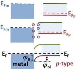
A Schottky barrier, named after Walter H. Schottky, is a potential energy barrier for electrons formed at a metal-semiconductor junction.Schottky barriers have rectifying characteristics, suitable for use as a diode.One of the primary characteristics of a Schottky barrier is the Schottky barrier height, denoted by Φ B (see figure). The value of Φ B depends on the combination of metal and ... Download scientific diagram | Energy band diagram of a metal-semiconductor Schottky diode with a p -doped quantum well, ͑ a ͒ without bias and ͑ b ͒ with forward bias. E c from publication ...
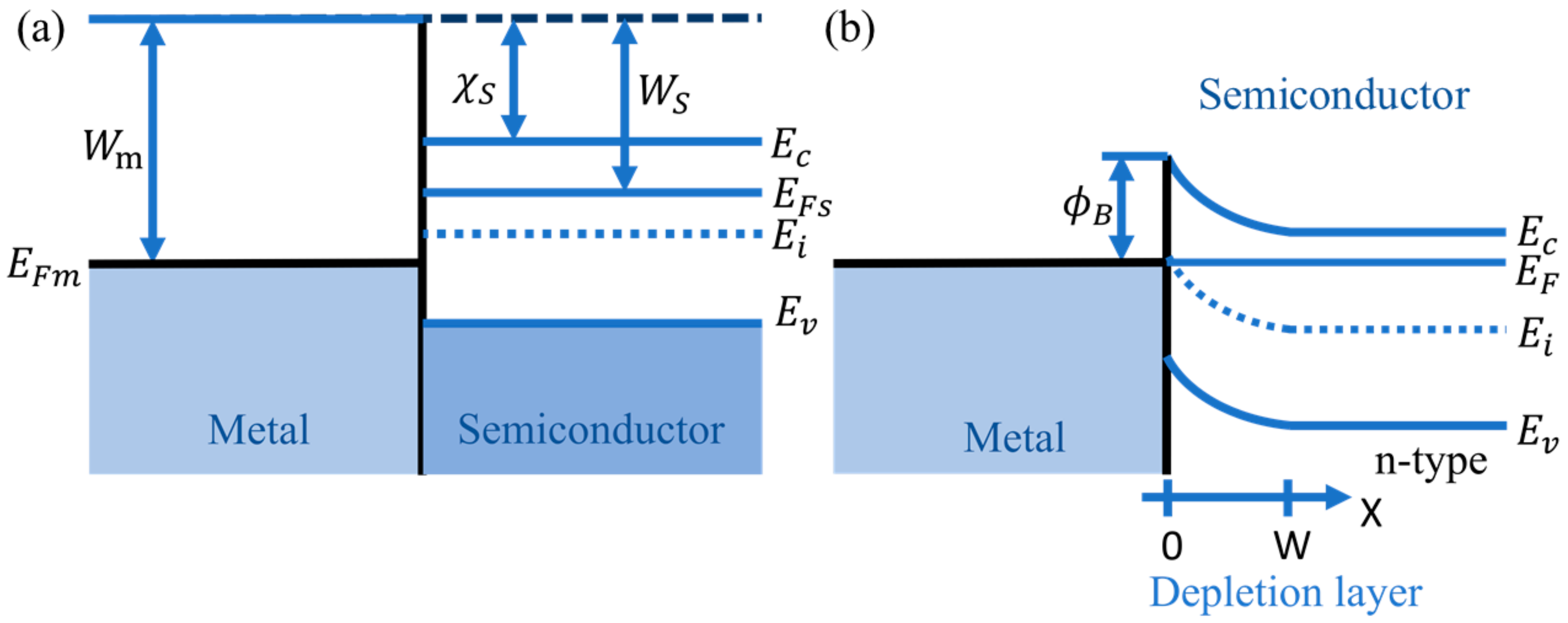
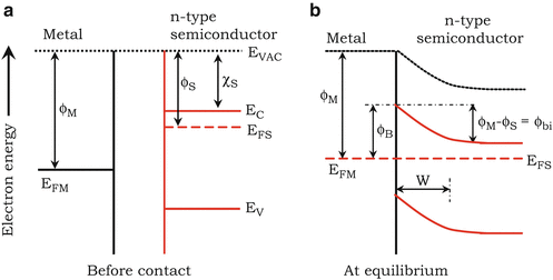
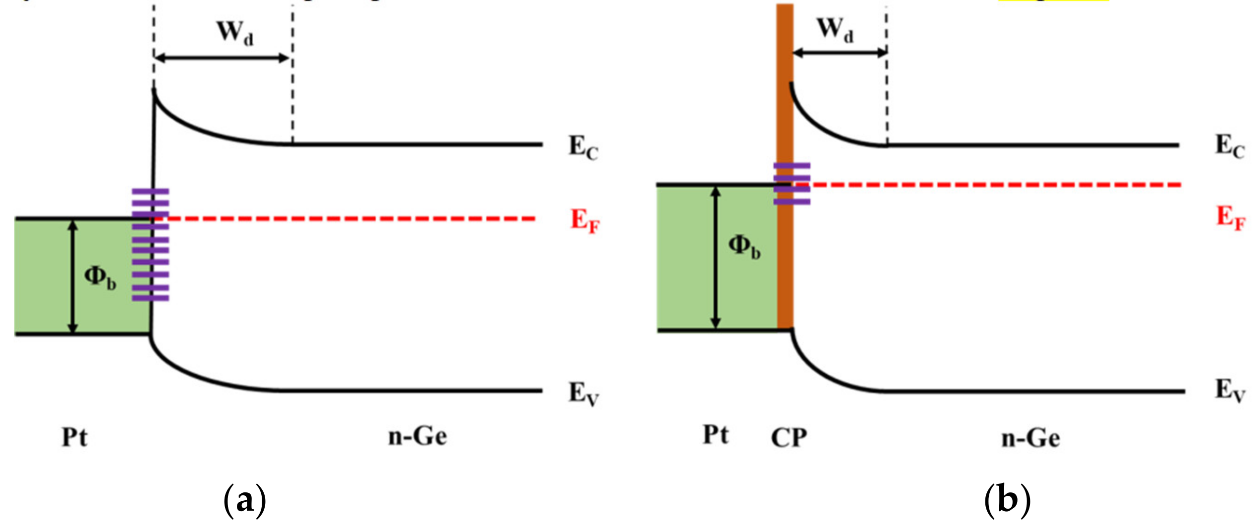
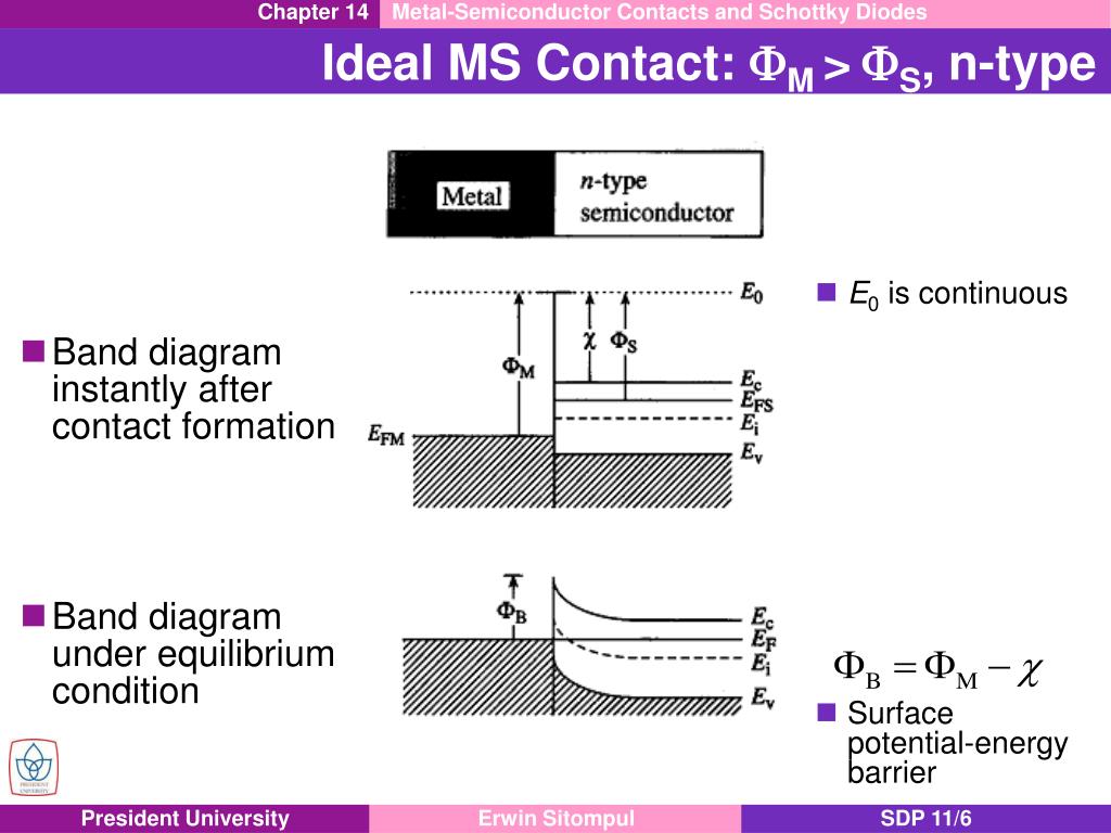
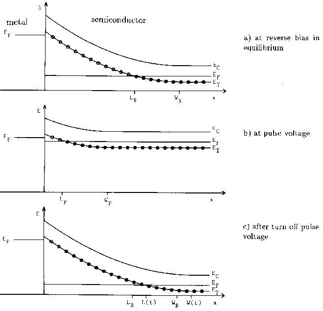
In a Schottky diode, the semiconductor band diagram looks very similar to that of an n-type semiconductor in a p +-n diode (compare Fig. 1a and 2). Hence, the variation of the space charge density, r , the electric field, F , and the potential, f , in the semiconductor near the metal-semiconductor interface can be found using the depletion ...
Schottky diode band diagram
Apr 22, 2011. #1. paul_harris77. 52. 0. Dear All. I am having problems with how to draw band diagrams with band bending for Schottky Barriers and PN junctions. My issue is that I don't know how you determine which Fermi level remains fixed at its equilibrium level and which Fermi level moves to align with it when the two materials are brought ... https://www.patreon.com/edmundsjIf you want to see more of these videos, or would like to say thanks for this one, the best way you can do that is by becomin... »Equilibrium band-diagram »DC Thermionic current (simple derivation) • 23.2 Physical Processes »DC Thermionic current (detailed derivation) ... Schottky barrier diode is a majority carrier device of great historical importance. There are similarities and differences with p-n junction diode: for
Schottky diode band diagram. The "turn on voltage" of a Schottky diode is typically smaller than a comparable p-n junction since the barrier to forward current flow ( m- s) is typically small. This "turn on" voltage can be as small as 0.3 Volts in some Si Schottky diodes. This makes a Schottky diode the best choice for power switch protection in inductive Figure 6 Band diagram showing the forward bias current through the diode. 6 Figure 7 Band diagram showing the reverse bias diode with built-in potential. 6 Figure 8 Ni on SiC Schottky diode Ar implantation; and I-V curve sketch. 9 Figure 9 Schottky contact with and without oxide layer edge guard. 10 Schottky diode, also known as Schottky barrier diode (SBD), fabricated on GaN and related III-Nitride materials has been researched intensively and extensively for the past two decades. This chapter reviews the property of GaN material, the advantage of GaN-based SBD, and the Schottky contact to GaN including current transporation theory, Schottky material selection, contact quality and ... and Schottky barrier diodes (SBDs) on different region of the same substrate have been developed to overcome the AC driving problems and achieving high breakdown voltage SBDs with high efficiency LEDs on the same wafer [1 - 7] .
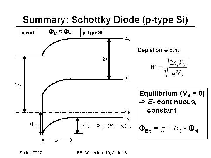
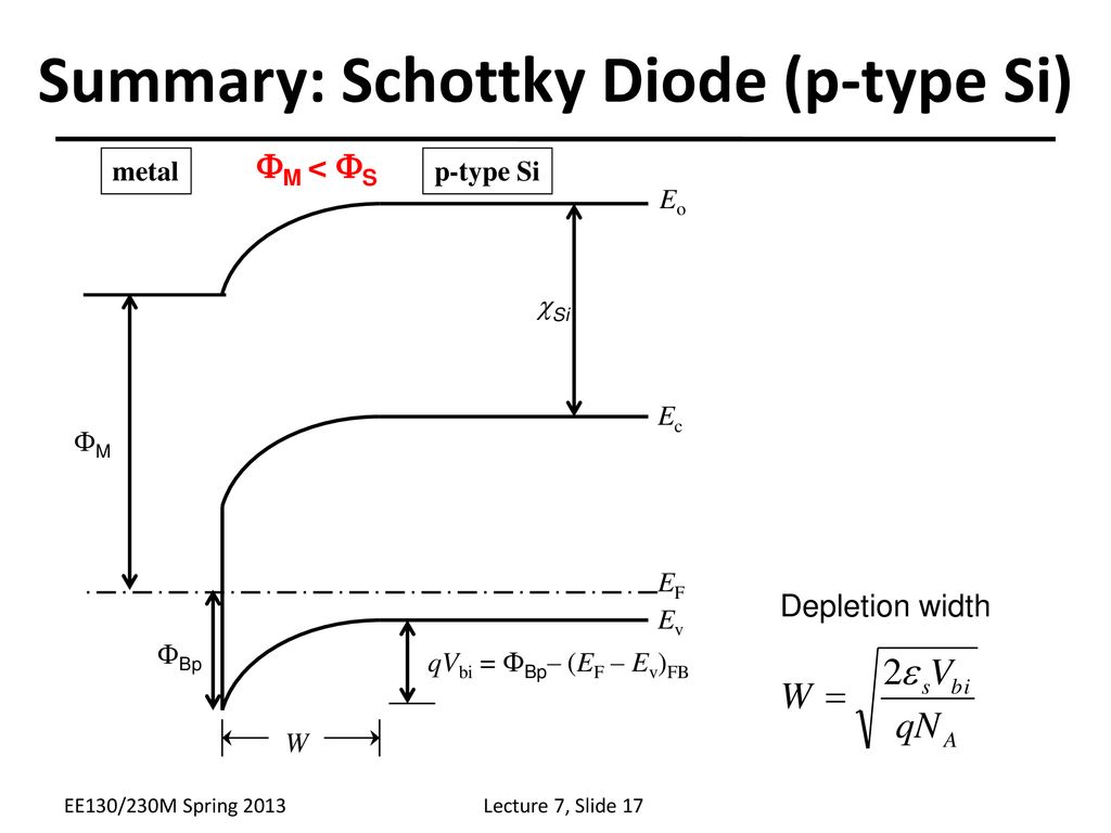
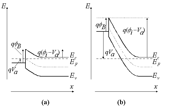
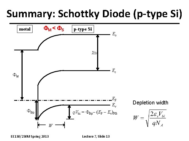
The Schottky diode (named after the German physicist Walter H. Schottky), also known as Schottky barrier diode or hot-carrier diode, is a semiconductor diode formed by the junction of a semiconductor with a metal. It has a low forward voltage drop and a very fast switching action. The cat's-whisker detectors used in the early days of wireless and metal rectifiers used in early power ... 4.1.1 Energy Band Diagram and Depletion Layer of a PN Junction ... They are called Schottky diodes and have some interesting applications.68 pages Schottky Diode. Schottky Diodes are formed by Metal Semiconductor Junctions [1] [2]. This junction is the root cause of the low turn on voltage of the devices [1] [2]. The physics surrounding the Schottky Diode and Ohmic Metal Semiconductor junctions will also be discussed in this report. 9.1 Schottky Barriers Energy Band Diagram of Schottky Contact • Schottky barrier height, φB, is a function of the metal material. • φB is the single most important parameter. The sum of qφBn and qφBp is equal to Eg. Metal Depletion layer Neutral region qφBn Ec Ec Ef Ef Ev qφ Ev Bp
2.2 Energy band diagram for Schottky contact after contact formation 15 2.3 Energy band diagram for a metal and n-type semiconductor with an interfacial layer between them 16 2.4 Response of bias voltage to a Schottky diode 18 2.5 Energy band diagram for an ohmic contact after contact formation 21 2.6 I-V curve for the ohmic contact structure 21 Download scientific diagram | Energy band diagrams for a Schottky-PN junction diode (SPND): (a) zero bias state, (b) forward bias state, and (c) reverse bias state. from publication: A New Type of ... Energy band diagram of the Schottky junction under forward bias is shown in figure 9. Thus, electrons injected from the external circuit into the n-type ...16 pages schottky diodes. Two main electrical characterization techniques were used in the investigation of these diodes, Current - Voltage Characterization and Capacitance - Voltage Characterization. Using I-V characteristics the ideality and the Barrier height of the Schottky diode was determined
Schottky diode Draw the band diagram (valence band, conduction band, Fermi energy) for a Schottky diode with a n doped semiconductor and a p doped semiconductor at zero bias. Assume that interface states pin the Fermi energy to the middle of the semiconducting gap at the interface. Indicate where the depletion region is and explain why it is depleted. ...

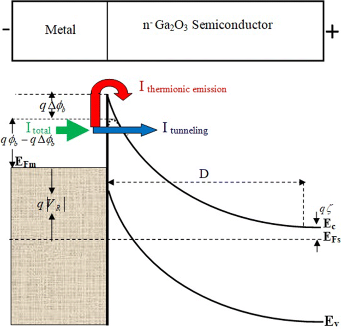
(A) Schematic structure of Schottky PD and (B) band diagram of metal/n-semiconductor Schottky contact. Schottky photodetectors are of many advantages such as a simple structure, easy to fabricate, a flat spectral response at short wavelength, no requirement for bias, and a relatively simple array readout circuit.
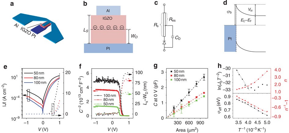
Simulation and Fabrication of Schottky Diodes and FETs based on IGZO Metal-Oxide Semiconductor A thesis submitted to the University of Manchester for the degree of ... Figure 1.2(a): Energy band diagrams for Schottky contact on n-type semiconductor and

Schottky Diode Structure Diagram. If the Schottky diode pin material is made of high-purity oxygen-free copper, which will improve the conductivity and thickness. It also has better conductivity and will not heat up for a long time. While the ordinary copper wire will be easily oxidized and soldered, resulting in low performance and easy ...

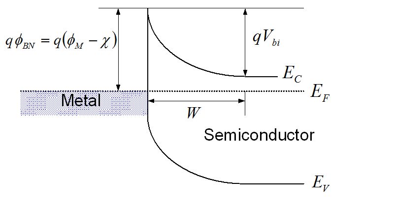
• Schottky Barrier/Diode ... Energy band diagram of an isolated metal adjacent to an isolated n-type semiconductor UMass Lowell 10.523 - Sanjeev Manohar. Energy band diagram of a metal-semiconductor contact in thermal equilibrium. UMass Lowell 10.523 - Sanjeev
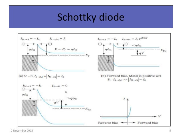
The Energy-band diagram versus voltage for the metal-semiconductor Junction shown in Fig.3 is very similar to these of the p-n junction. Because of similarity, we expect the current-voltage characteristics of the Schottky barrier junction to be similar to the exponential behavior of the p-n junction diode.
3. 1. 6. 2 Schottky Contact A Schottky barrier refers to a metal-semiconductor contact having a large barrier height (i.e. and low doping concentration that is less than the density of states in the conduction band or valence band. The potential barrier between the metal and the semiconductor can be identified on an energy band diagram.
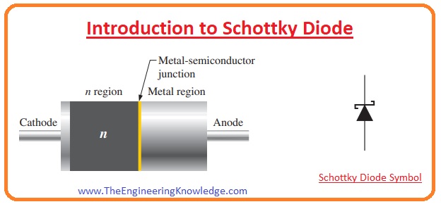
The schottky diode is a type of metal - semiconductor junction diode, which is also known as hot-carrier diode, low voltage diode or schottky barrier diode. The schottky diode is formed by the junction of a semiconductor with a metal. Schottky diode offers fast switching action and has a low forward voltage drop.
Schottky diode Draw the band diagram (valence band, conduction band, Fermi energy) for a Schottky diode with a n doped semiconductor and a p doped semiconductor at zero bias. Assume that interface states pin the Fermi energy to the middle of the semiconducting gap at the interface.
Let's see the diagram of the energy band of Schottky diode: Schottky diode Characteristics Curve. Now, let's discuss the voltage and current characteristics of the Schottky diode. It has low forward voltage loss that's why its characteristic curve is close to current axes as compared to normal diodes.
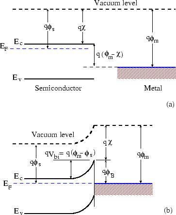
The Schottky diodes are also called hot-carrier diode, ... Schottky Diode Energy Band. In the below figure energy band diagram for N-type semiconductor material and metallic material is shown below. The energy level of electrons at the outer side of the substance is known as the vacuum level.
Energy band diagram of schottky diode. The energy band diagram of the N-type semiconductor and metal is shown in the below figure. The vacuum level is defined as the energy level of electrons that are outside the material. The work function is defined as the energy required to move an electron from ...

Energy band diagram and carrier activity at \(V_A < 0\) \(I-V\) Characteristics In general, the current flowing through the Schottky contact can be defined with the applied voltage, which is very similar to those of pn-junction diode.
»Equilibrium band-diagram »DC Thermionic current (simple derivation) • 23.2 Physical Processes »DC Thermionic current (detailed derivation) ... Schottky barrier diode is a majority carrier device of great historical importance. There are similarities and differences with p-n junction diode: for
https://www.patreon.com/edmundsjIf you want to see more of these videos, or would like to say thanks for this one, the best way you can do that is by becomin...

Apr 22, 2011. #1. paul_harris77. 52. 0. Dear All. I am having problems with how to draw band diagrams with band bending for Schottky Barriers and PN junctions. My issue is that I don't know how you determine which Fermi level remains fixed at its equilibrium level and which Fermi level moves to align with it when the two materials are brought ...


0 Response to "44 schottky diode band diagram"
Post a Comment